What is the process for manufacturing semiconductors?
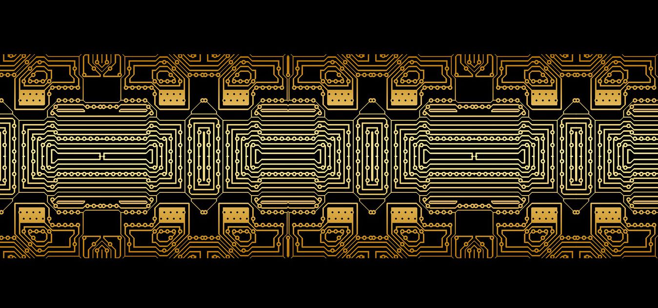
Photolithography is the process used to fabricate semiconductor devices. It is a process by which a pattern is transferred from a photomask to the surface of a wafer. It is the most time-consuming and, as a rule, the most complicated process.
Transistors are now getting smaller and manufacturers cannot build them using normal methods. This is why photolithography solves this problem without the need to move complex machinery very precisely by using light as the etching method. This pattern transfer is aimed at limiting very fine or high resolution areas or geometries in the integrated circuit to be manufactured and is performed in the clean room.
Photolithography is also called optical lithography or UV lithography, as it uses light to model parts of a thin film and transfer a geometric pattern from a chemical photoresist that is sensitive to light.
There are not many manufacturers that can create such advanced chips. In essence, a chip is a device that incorporates in a single piece of semiconductor all the elements of a printed circuit. Although it is true that it does not matter much if the transistors are made so small that they do not work, because they form the so-called quantum tunnel, that is, electricity continues to pass even when it is turned off.
The photolithography process combines several steps in sequence, the steps of this process are:
1. Cleaning of semiconductor wafers: remove any type of contaminant from the surface.
2. Silicon oxidation: creating a SiO2 layer that acts as a protective layer on the surface and as an electrical insulator.
3. Application of the photoresin: the surface is covered with a light-sensitive substance, leaving the wafer coated with a flat, uniform layer.
4. Exposure and development of the photoresist: the wafer is exposed to ultraviolet light and the photoresist is illuminated through the areas not obscured by the pattern drawn on the mask. Subsequently the wafer is "softened" in the illuminated parts by subjecting it to a chemical agent that removes the illuminated areas.
5. Etching: selective etching process of the silicon wafer in those areas that have not been protected by the photoresist.
6. Elimination of photoresin: through a process of dissolution and elimination when it is no longer necessary.
Inelmatic selects semiconductors from leading manufacturers to offer a longer life cycle and far superior durability than cheaper suppliers. For more information, please consult our experts.